Using KStep
- Configuring KFLOP/Kogna for use with KStep
- Enable KStep Amplifiers
- Digital Status
- Relay Driver Outputs
- Connecting and Using 2 KSteps
- Analog Output
KStep is a high efficiency 4-axis microstepping drive that can drive four motors with up to 5Amps @ 48V each. In addition to the 4 motor drives, KStep also provides additional I/O features:
- Sixteen (16) 12-24V tolerant optically isolated filtered inputs
- Two (2) optically isolated relay driver type outputs, each good for 0.1A @ 30V
- One (1) isolated PMW to Analog output
All controller signals are 3.3V/LVTTL compatible. An on-board voltage clamp circuit to protect against regenerative over voltage is also included. KStep is designed to snap together with KFLOP/Kogna for easy plug and play operation. A single 26-pin ribbon cable provides all the logic, power, Step/Dir Signals, Enable, Relay driver, Analog PWM, and Optically isolated input connections between the KStep and KFLOP/Kogna boards. If necessary, two KSteps can be connected to a single KFLOP/Kogna to drive a total of 8 motors.

Figure 1 - KStep

Figure 2 - KStep + KFLOP
Configuring KFLOP/Kogna for use with KStep
Configuring KStep is fairly straightforward, as it is normally used in an open loop system (although it is possible to operate in closed loop stepper mode) so all feedback, servo, PID, Filter, Feedforward and commutation parameters are not used and can be ignored. KStep is effectively a Step/Dir driver, so it makes use of the Step/Dir Output mode in KFLOP/Kogna (See the items circled in red below - Note that output mode type "Step Dir" is selected). The screen shown is the Output Channel selection for KStep Motor channel #0. Note that output channel 8 is selected instead of 0 as you might assume. As KStep requires a LVTTL signal, rather than using Output channels 0 through 4, Output channels 8 through 11 respectively should be used instead, as they provide a LVTTL signal. See here for more information. An output gain of -1 may be specified to reverse the direction of motion.
Note: for the pulse polarity and pulse time to be set properly, the following line of C Code needs to be executed after every power up:
FPGA(STEP_PULSE_LENGTH_ADD) = 63 + 0x80; // set polarity and pulse length to 4μs
When using the default settings, there is marginal timing on direction setup which may result in "drift" caused by a microstep in the wrong direction when changing directions. This line of Code is already included in the Example C Initialization Programs (i.e. InitKStep3Axis.c):
FPGA(STEP_PULSE_LENGTH_ADD) = 63 + 0x80; // set polarity and pulse length to 4μs
Example Axis configurations are also provided as KStepAxis0.mot, KStepAxis1.mot, KStepAxis2.mot, KStepAxis3.mot

Example Axis configurations are provided in the C:\KMotion431\KMotion\Motors directory (assuming a default install location). KStepAxis0.mot, KStepAxis1.mot, KStepAxis2.mot and KStepAxis3.mot are the most basic configurations. Limit switch options are also configured on this screen. KStep's optically isolated 12-24V Inputs are commonly used to connect Limit switches and are referenced as Input Bits 168 through 183 inclusive. If you are using NC (normally closed) type limit switches, this means that the inputs are normally high and become low when activated. In this case the "Stop when low" option should be selected. If using NO (normally open) type limit switches, this means the inputs are normally low, and become high when activated. In this case, the "Stop when low" option should be cleared. For more info see here.

Motion profile settings on the Step Response Screen are used.

Enable KStep Amplifiers
An amplifier enable signal is required to enable the KStep Full Bridge Amplifiers. One signal enables all four of the KStep amplifiers. The enable signal is positive true, meaning the drives are enabled when a 3.3V LVTTL (sourcing) signal is received. When using a 26-pin ribbon cable to connect KStep (JP 36) and KFLOP/Kogna (JP 7), this signal is routed to KFLOP's IO 45, which must be set as an output, and also set high to enable the drives. Note that the enable signal is only optically isolated from VBB and GND when KStep is in isolated mode.
If JP36 is not being used to connect KFLOP/Kogna to KStep, then a 3.3V enable signal may be applied to a screw terminal on J6 instead. If two KSteps are being used (for driving 8 motors), then the screw terminals on J6 should be used as an output on the first KStep to daisy chain the enable signal to the second KStep.
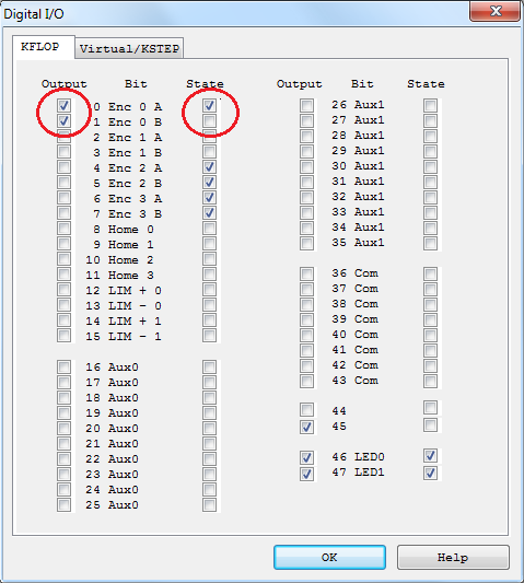
For testing purposes KStep may be enabled using the Digital I/O Screen as shown below.

From C code the Amplifiers can be enabled with the following code:
	SetBitDirection(45,1); 	// set Enable Signal as Output
	SetBit(45); 			// Enable the KStep Amplifiers
It's possible to write code to enable the amplifiers as soon as motion is detected and disabled after a period of time with no motion. Here is an example:
	double T0, LastX=0, LastY=0, LastZ=0;
	for (;;) 	// loop forever
	{
		WaitNextTimeSlice();

		// Service Amplifier disable after no activity for a while
		if (ch0->Dest != LastX || ch1->Dest != LastY || ch2->Dest != LastZ)
		{
			// we moved - enable KStep Amplifers>
			SetBit(45);
			T0 = Time_sec(); 	// record the time and position of last motion<
			LastX=ch0->Dest;
			LastY=ch1->Dest;
			LastZ=ch2->Dest;
		}
		else
		{
			if (Time_sec() > T0 + 10.0) ClearBit(45);
		}
	}
Digital Status
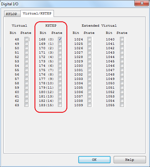
The state of the Optically Isolated 12-24V Digital Inputs can be observed by selecting the "Virtual/KStep" Tab on the Digital I/O Screen. Each input will be marked as active if current is flowing through the optical isolation circuit. For input circuits and pinouts see. The KStep Opto Inputs are actually virtual inputs that are multiplexed in through KFLOP/Kogna I/O. KFLOP/Kogna can perform this multiplexing automatically by setting the global variable KStepPresent. The following line of C code should be added to your Init.c program:
KStepPresent=TRUE;

Relay Driver Outputs
The Optically Isolated 24V outputs can be observed and controlled by selecting the KFLOP/Kogna tab on the Digital I/O Screen. Each output will be marked as active if current is flowing through the optical isolation circuit. The KStep outputs are the same as the standard KFLOP/Kogna outputs except they are optically isolated and amplified to handle up to 24V. For output circuit and pinouts see Relay Driver Outputs.

To make use of the outputs within a C program the following C code shows an example of enabling both the outputs, turning them on, then turning them off.
		SetBitDirection(0,1);	//set as output
		SetBitDirection(1,1);	//set as output

		SetBit(0);	// turn output on
		SetBit(1); 	// turn output on

		ClearBit(0); 	// turn output of
		ClearBit(1); 	// turn output off
Connecting and Using 2 KSteps
Connect the RJ45 cable between KFLOP/Kogna JP5 and KStep#2 JP26. KFLOP's/Kogna's Step/Dir Generators 4-7 will then be connected to KStep#2. Configure as OutputChan0 12-15 to drive in TTL mode as required by KStep.
You will also need to provide power, GND, and Enable to KStep. The simplest method is usually to connect the 4 pins on J6 between the 2 KSteps. See Connecting and using 2 KSteps.
Analog Output
The KStep Analog output is a low Speed (10ms time constant) isolated analog output that is commonly used as a VFD Spindle Speed Control signal. KFLOP/Kogna outputs a 3.3V digital PWM on IO 44 to KStep which optically isolates and filters it to create an analog signal. Isolated power and ground (often supplied by the VFD) are required. The analog output voltage will be a proportion of the supplied voltage relative to the duty cycle of the PWM signal. For example a 75% high duty cycle will provide a voltage which is approximately 75% of the supplied voltage.
To configure KFLOP/Kogna to output the appropriate PWM signal into KStep the configuration code below should be used. There is an FPGA option to move PWM0 (which normally is output on connector JP6 with the other 7 PWM outputs) over to JP7 Pin5 IO 44. IO 44 must be configured as an output; the PWM Prescale dividers set to a reasonable value, and then enable PWM.
		FPGA(KAN_TRIG_REG)=4; 			// Mux PWM0 to JP7 Pin5 IO 44 for KStep
		SetBitDirection(44,1); 			// define bit as an output
		FPGA(IO_PWMS_PRESCALE) = 46;	// divide clock by 46 (1.4 KHz)
		FPGA(IO_PWMS+1) = 1;  			// Enable
The Analog output has nonlinearity near the 0% duty cycle region due to opto coupler pulse shaping effects. The nonlinearity can be mostly corrected in software through calibration. Below is a raw uncorrected analog output with a PWM frequency of 1.4KHz (PWM Prescale = 46).

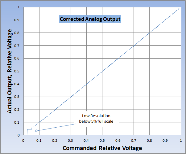
Using a correction algorithm where the PWM value that will most closely produce the desired output voltage is determined from a table lookup approach for the first 7 PWM counts, and a simple linear interpolation is used for determining PWM settings 7 through 240 the linearized results are shown below. Although the signal is now linear, the resolution is low for settings below ~5% full scale.

Below is the C function used to linearize the output.
	// PWM->Analog Correction
	//
	// assume very non-linear for first few count and linear thereafter
	//
	// Measure output ratio for first 0-7 counts then at 240

	float V[]=
	{
	0.001,	// count = 0
	0.031,	// count = 1
	0.044,	// count = 2
	0.054,	// count = 3
	0.062,	// count = 4
	0.069,	// count = 5
	0.074,	// count = 6
	0.079	// count = 7
	;

	float V240=0.970;

	int CorrectAnalog(float v)
	{
		int r;
		float v2=2.0f*v;
		// compare with half way points to determine closest count
		if (v2 < V[1]+V[0]) return 0;
		if (v2 < V[2]+V[1]) return 1;
		if (v2 < V[3]+V[2]) return 2;
		if (v2 < V[4]+V[3]) return 3;
		if (v2 < V[5]+V[4]) return 4;
		if (v2 < V[6]+V[5]) return 5;
		if (v2 < V[7]+V[6]) return 6;
		// must be 7 or higher do linear interpolation

		r = (int<)(7.5 + (v-V[7])/(V240-V[7])*(240.0f-7.0f));
		if (r>255) r=255;
		return< r;

}