KMotion - Connector Pinouts
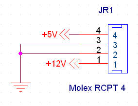
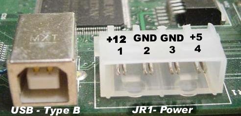
JR1 - 5V Power (regulated +/- 5%)
Typical current = 0.7Amps with no user I/O connected. More current may be required dependent on the amount of Digital I/O and Analog +/- 15V consumed by the user. Up to 2 watts of +/-15 volts is generated on board from this 5V supply (most of which is available for external use). 5V @ 2.5A should be more than sufficient under all conditions. The 12V input is not used internally by the board, but is routed to pins on the 37pin DB Motor connector and the 16 pin Aux Connector for the convenience of the user. 5V power is also routed to the 37pin DB Motor connector, 5V power may be applied at whichever connector is more convenient. This connector is only rated for 6.5Amps per connection, if more total motor current is required, power should be externally routed to the 37pin DB Supply 0-3 inputs directly.
This connector is a standard PC-disk drive power connector which makes it easy to drive the board and small to medium size motors (< 12V) with an inexpensive PC power supply and very few external connections. Simply plug the PC power supply here, jumper the +12V signals on the DB37 Pin connector to the desired motor supply inputs, and connect your motors.
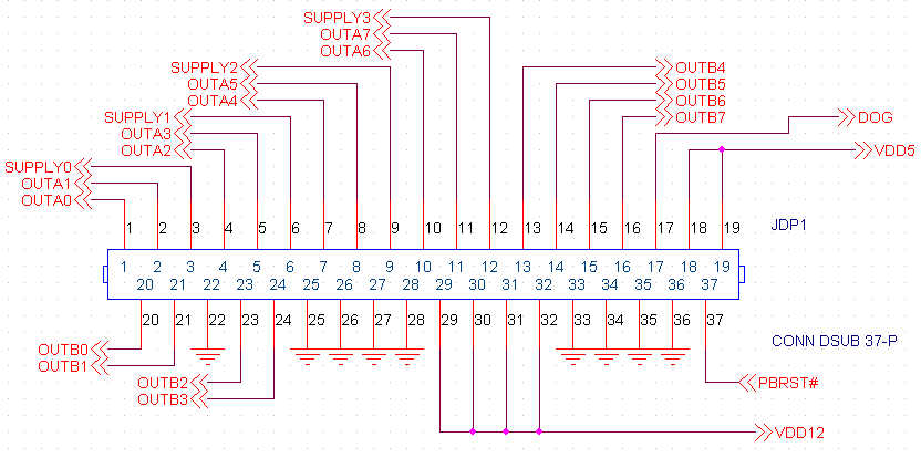
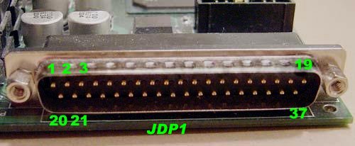
JDP1 - Motor/Motor Supply (12-55V) Connector
The KMotion motion control board is basically a 4 axis Motor controller that consists of 8 full bridge drivers (see figure 1). A full bridge driver is able to apply a positive or negative voltage to a load using only a single positive supply. The load is connected across the OUTA and OUTB terminals. The 8 full bridge drivers are grouped into 4 pairs, where a pair of full bridge drivers are associated with a motor axis. This is because some types of motors (stepper motors or 3-phase motors require more than a single full bridge to drive them).

Each axis (and pair of full bridge drivers) share a common power supply pin, heat sink, encoder input, and current sense circuitry. Each axis may be of a different type (DC-Brush, 3-phase brushless, or stepper) and may use a different supply voltage (12-55V DC). If a DC-Brush motor is used for an axis only one of the full bridge drivers are used, the other is left unconnected. 3-phase brushless motors use 1½ full bridges (3 - half bridges), and stepper motors have 2 coils which require both full bridges.
| Motor type DC -Brush | Motor type - 3 Phase brushless | Motor type - Stepper | |
|---|---|---|---|
| Axis 0 | Connect Motor across OUTA0-OUTB0 Leave OUTA1-OUTB1 disconnected |
Connect Phase A to OUTA0 Connect Phase B to OUTB0 Connect Phase C to OUTA1 Leave OUTB1 disconnected |
Connect Coil A across OUTA0-OUTB0 Connect Coil B across OUTA1-OUTB1 |
| Axis 1 | Connect Motor across OUTA2-OUTB2 Leave OUTA3-OUTB3 disconnected |
Connect Phase A to OUTA2 Connect Phase B to OUTB2 Connect Phase C to OUTA3 Leave OUTB3 disconnected |
Connect Coil A across OUTA2-OUTB2 Connect Coil B across OUTA3-OUTB3 |
| Axis 2 | Connect Motor across OUTA4-OUTB4 Leave OUTA5-OUTB5 disconnected |
Connect Phase A to OUTA4
Connect Phase B to OUTB4 Connect Phase C to OUTA5 Leave OUTB5 disconnected |
Connect Coil A across OUTA4-OUTB4 Connect Coil B across OUTA5-OUTB5 |
| Axis 3 | Connect Motor across OUTA6-OUTB6 Leave OUTA7-OUTB7 disconnected |
Connect Phase A to OUTA6
Connect Phase B to OUTB6 Connect Phase C to OUTA7 Leave OUTB7 disconnected |
Connect Coil A across OUTA6-OUTB6 Connect Coil B across OUTA7-OUTB7 |
Also available on this connector is PBRST#. Short PBRST# to ground to reset the board. This signal is internally de-bounced. Under normal conditions, on-board power up reset should suffice so this pin may be left disconnected. Also connecting this pin to the DOG pin will enable the on board watchdog circuitry, whenever there is no DSP/FPGA activity detected for 1 second the board will be automatically reset. This is not normally required and may be left disconnected.
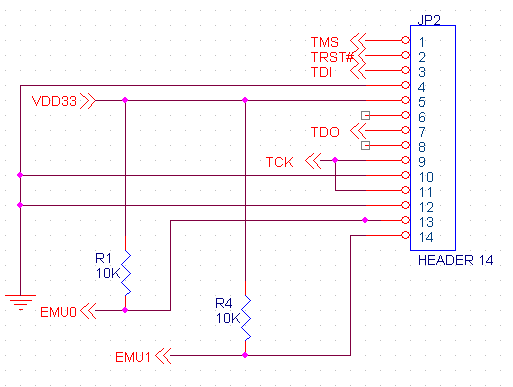
JP2 - JTAG
This connector is only used for advanced debugging using an XDS510 JTAG in circuit emulator. A small amount of regulated 3.3V (<0.5 Amp) is available on this connector if needed for external use.
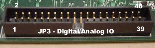
JP3 - Digital/Analog IO
4 channels of +/- 10V analog inputs, 4 channels of +/- 10V analog outputs, 4 channels of 0-4V analog outputs, 22 LVTTL bi-directional digital I/O, and +5, +15, -15 power supply outputs. Many Digital I/O bits are pre-defined as encoder, home, or limit inputs (see table below) but if not required for the particular application may be used as general purpose I/O. Digital Outputs may sink/source 10 ma. Digital I/O is LVTTL (3.3V) but is 5 V tolerant.
Caution! This connector contains +/- 15 v signals. Shorts to low voltage pins are likely to cause permanent damage to the board!
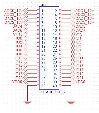
| Pin | Name | Description |
|---|---|---|
| 1 | ADC0_10V | ADC Chan 0 +/- 10V input |
| 2 | ADC1_10V | ADC Chan 1 +/- 10V input |
| 3 | ADC2_10V | ADC Chan 2 +/- 10V input |
| 4 | ADC3_10V | ADC Chan 3 +/- 10V input |
| 5 | DAC0_10V | DAC Chan 0 +/- 10V output |
| 6 | DAC1_10V | DAC Chan 1 +/- 10V output |
| 7 | DAC2_10V | DAC Chan 2 +/- 10V output |
| 8 | DAC3_10V | DAC Chan 3 +/- 10V output |
| 9 | DAC4 | DAC Chan 4 0-4V output |
| 10 | DAC5 | DAC Chan 5 0-4V output |
| 11 | DAC6 | DAC Chan 6 0-4V output |
| 12 | DAC7 | DAC Chan 7 0-4V output |
| 13 | VM15 | -15V @ 0.07 Amps Output |
| 14 | V15 | +15V @ 0.07 Amps Output |
| 15 | IO0 | Gen Purpose LVTTL I/O or Axis 0 Encoder Input Phase A |
| 16 | IO1 | Gen Purpose LVTTL I/O or Axis 0 Encoder Input Phase B |
| 17 | IO2 | Gen Purpose LVTTL I/O or Axis 1 Encoder Input Phase A |
| 18 | IO3 | Gen Purpose LVTTL I/O or Axis 1 Encoder Input Phase B |
| 19 | IO4 | Gen Purpose LVTTL I/O or Axis 2 Encoder Input Phase A |
| 20 | IO5 | Gen Purpose LVTTL I/O or Axis 2 Encoder Input Phase B |
| 21 | IO6 | Gen Purpose LVTTL I/O or Axis 3 Encoder Input Phase A |
| 22 | IO7 | Gen Purpose LVTTL I/O or Axis 3 Encoder Input Phase B |
| 23 | IO8 | Gen Purpose LVTTL I/O or Axis 0 Home or Step 0 output |
| 24 | IO9 | Gen Purpose LVTTL I/O or Axis 1 Home or Dir 0 output |
| 25 | IO10 | Gen Purpose LVTTL I/O or Axis 2 Home or Step 1 output |
| 26 | IO11 | Gen Purpose LVTTL I/O or Axis 3 Home or Dir 1 output |
| 27 | IO12 | Gen Purpose LVTTL I/O or Axis 0 + Limit or Step 2 output |
| 28 | IO13 | Gen Purpose LVTTL I/O or Axis 0 - Limit or Dir 2 output |
| 29 | IO14 | Gen Purpose LVTTL I/O or Axis 1 + Limit or Step 3 output |
| 30 | IO15 | Gen Purpose LVTTL I/O or Axis 1 - Limit or Dir 3 output |
| 31 | IO16 | Gen Purpose LVTTL I/O or Axis 2 + Limit |
| 32 | IO17 | Gen Purpose LVTTL I/O or Axis 2 - Limit |
| 33 | IO18 | Gen Purpose LVTTL I/O or Axis 3 + Limit |
| 34 | IO19 | Gen Purpose LVTTL I/O or Axis 3 - Limit |
| 35 | IO20 | Gen Purpose LVTTL I/O |
| 36 | IO21 | Gen Purpose LVTTL I/O |
| 37 | VDD5 | +5 Volts Output |
| 38 | VDD5 | +5 Volts Output |
| 39 | GND | Digital and Analog Ground |
| 40 | GND | Digital and Analog Ground |
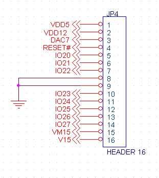
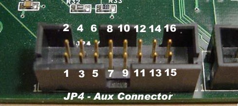
JP4 - Aux Connector
Auxiliary connector which supplies power, reset, one 0-4V DAC, and 8 digital I/O normally connected to optional expansion daughter boards. If no expansion module is required these digital I/O may be used for general purpose use. Note: IO20 and IO21 are also routed to JP3
| Pin | Name | Description |
|---|---|---|
| 1 | VDD5 | +5 Volts Output |
| 2 | VDD12 | +12 Volts Output |
| 3 | DAC7 | DAC Chan 7 0-4V output |
| 4 | RESET# | Power up Reset (low true) output |
| 5 | IO20 | Gen Purpose LVTTL I/O |
| 6 | IO21 | Gen Purpose LVTTL I/O |
| 7 | IO22 | Gen Purpose LVTTL I/O |
| 8 | GND | Digital and Analog Ground |
| 9 | GND | Digital and Analog Ground |
| 10 | IO23 | Gen Purpose LVTTL I/O |
| 11 | IO24 | Gen Purpose LVTTL I/O |
| 12 | IO25 | Gen Purpose LVTTL I/O |
| 13 | IO26 | Gen Purpose LVTTL I/O |
| 14 | IO27 | Gen Purpose LVTTL I/O |
| 15 | VM15 | -15V @ 0.07 Amps Output |
| 16 | V15 | +15V @ 0.07 Amps Output |
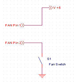
Fan and Aux Switches
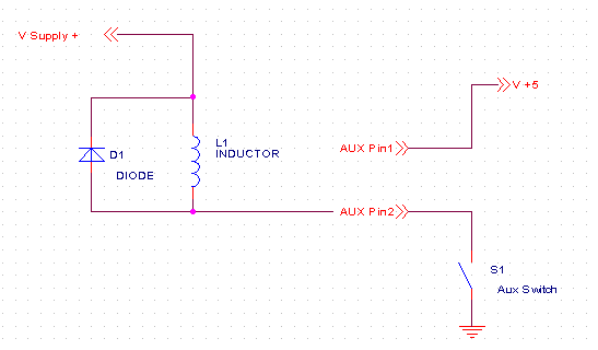
Kmotion contains two SPST switches to ground capable of driving up to 30V @ 2A. One is dedicated to driving the cooling fan and one is available for another use. If the fan is not required by the application (less than 2Amps drawn on all axis) it may also be used to drive an external load. Each of the switches is connected to a 2 pin connector. One of the pins is connected to the 5V supply and the other pin is switched to ground. If the load requires 5V (i.e.. a 5V fan) it may be connected directly across the 2 pins. If other than a 5V load is required, then external user supplied wiring to the supply is required and only the pin that is switched to ground should be connected. See below.
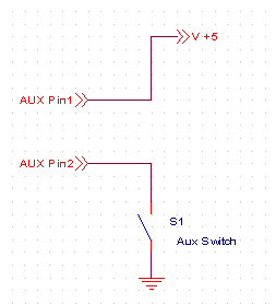
Here is an example of how a solenoid may be driven with the Auxiliary Switch:
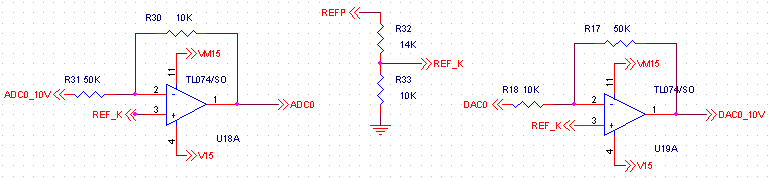
Analog I/O circuit
Circuit diagram of analog I/O buffers showing conversion from industry standard +/- 10V ranges to onboard 0-4V ADC/DAC converters. Note 50K input impedance. REFP = 4V, REFK = 1.43V